SPUTTERING TARGETS & BONDING EXPERTISE

From material selection to finished bonded assemblies, covering every stage of your project.

6N Purity up to 99.9999% for semiconductor processes.
100% Inspection and full 
lot traceability.
<1% Scrap rate through
void-free bonding.
2 Dedicated bonding facilities with
proprietary pre-wetting technology.

ENGINEERED FOR YOUR DEPOSITION PROCESS

Repeatable layers, run after run.
 Compatible with EVATEC, AMAT, ANELVA, SPTS, UNAXIS and other major PVD platforms.

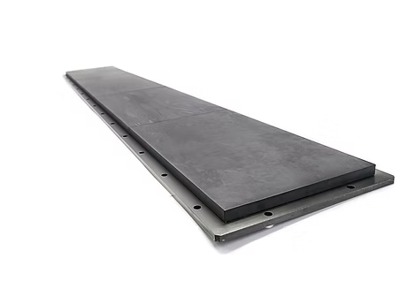
STANDARD SPUTTERING TARGETS

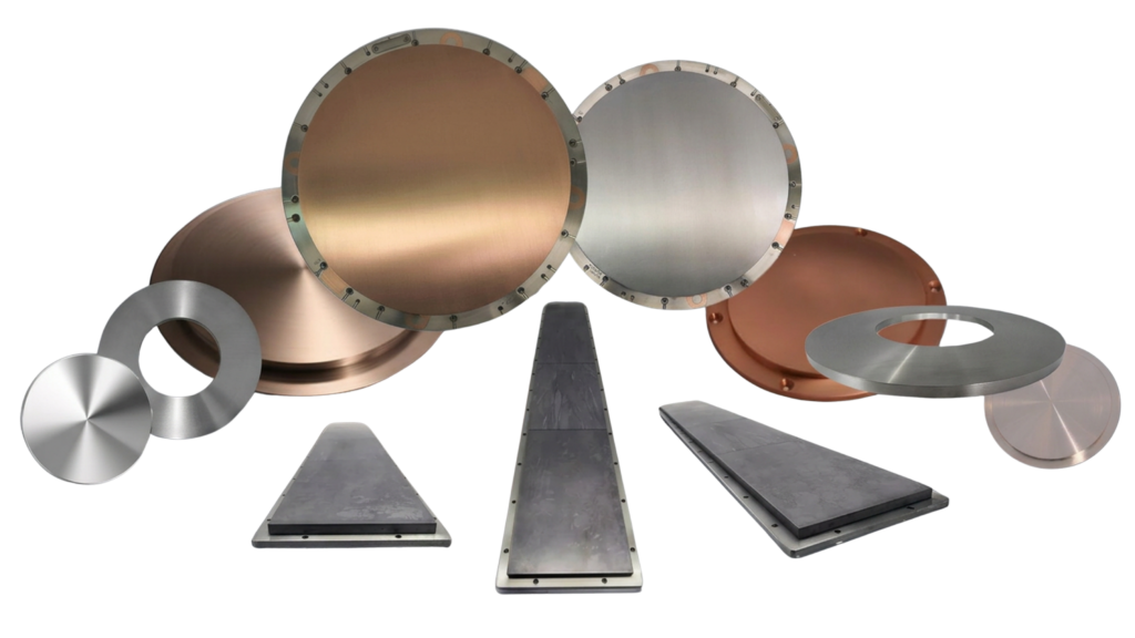
Planar and rotatable targets for optical, decorative, wear-resistant and functional coatings in standard and custom configurations.
HIGH-PURITY MATERIALS

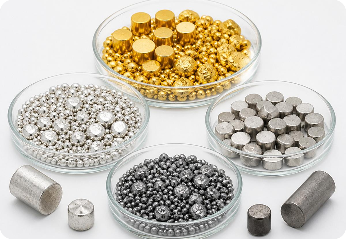
Semiconductor-grade sputtering targets and evaporation materials with certified analysis 
 for every order.
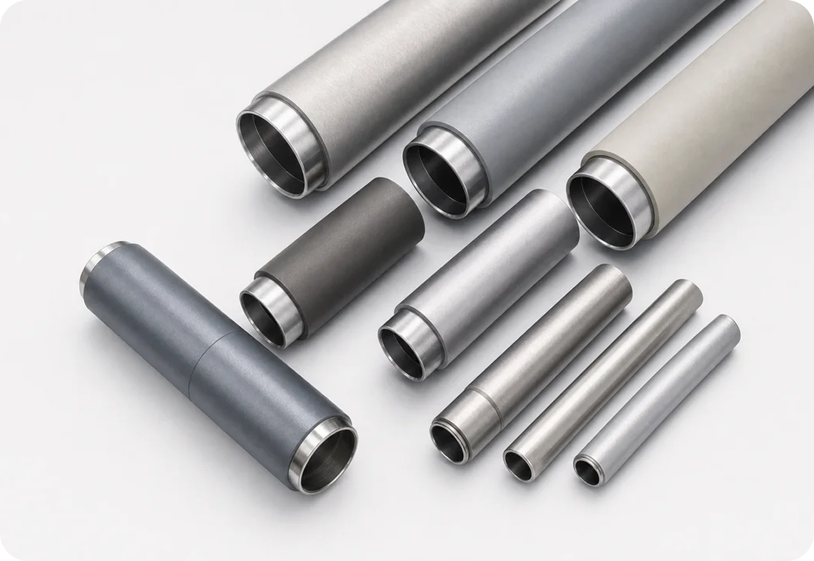
ROTATABLE CONFIGURATIONS

Monolithic, sprayed and bonded rotatable tubes developed for higher target utilization, longer campaign life and reliable process performance.
WHAT YOU GAIN

Shorter
qualification cycles

Reliable
process performance

Fast
turnaround

Dedicated
technical support

OEM
compatibility

SPUTTERING TARGETS AND EVAPORATION MATERIALS

STANDARD SPUTTERING TARGETS

  • Si ≥99.999% planar / 
≥99.9% rotatable
  • Nb ≥99.9% planar & rotatable
  • Ta ≥99.95% planar & rotatable
  • Al ≥99.99% planar & rotatable
  • Ti ≥99.99% planar & rotatable

HIGH-PURITY MATERIALS

  • Al, Al/Cu, Al/Si 99.95% – 99.999%
  • Cu 99.99% – 99.999%
  • Ti 99.99% – 99.995%
  • NiV 99.999% – 99.9995%
  • Ta 99.995% – 99.999%
  • WTi, Cr, Ge, W, Ni

PRECIOUS MATERIALS

  • Au 99.99% – 99.999%
  • Ag 99.99% – 99.999%
  • Pt 99.99% – 99.999%
  • Ru 99.95% – 99.99%

Additional metals, alloys, oxides and fluorides available on request in a wide range of shapes and purities.

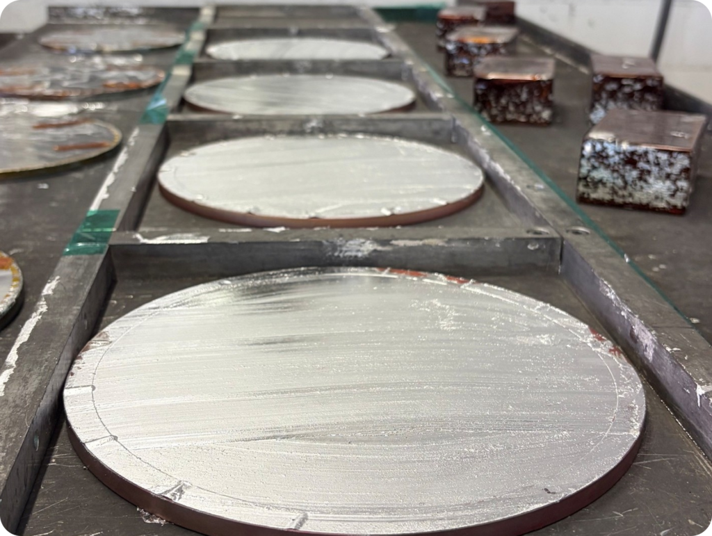
PROPRIETARY IN-HOUSE BONDING TECHNOLOGY

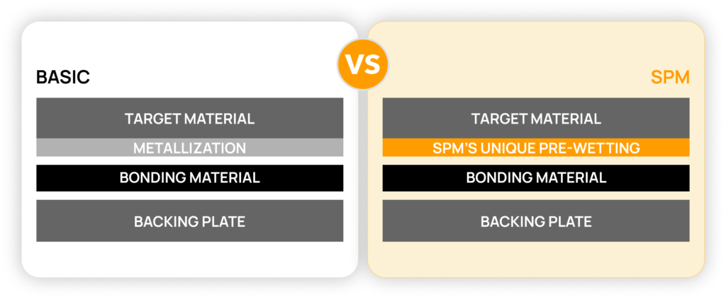
Developed in Japan, SPM’s proprietary pre-wetting process is material-independent and requires no metallization, delivering stable, void-free bonds.

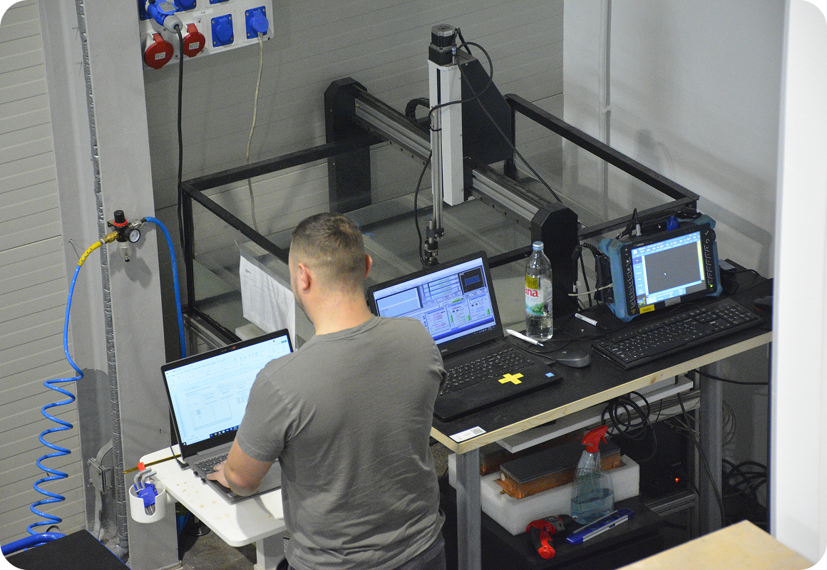
Ultrasonic verification

Void-free bonding

No metallization

<1% scrap rate​

Thin-film uniformity​

RELIABILITY YOU CAN VERIFY

Supporting stable deposition from qualification to production.

INSPECTION & DOCUMENTATION

Dimensional, purity and ultrasonic bond verification with certificates for each delivery.

BUILT TO YOUR SPECIFICATION

Custom geometries, alloy development, prototype quantities and small production runs.

PROCESS SUPPORT

Application engineering for deposition rate, uniformity, arcing and target life improvement.
TARGET RECYCLING AND SCRAP MANAGEMENT

Recover value from spent targets through buy-back, rebonding and material recycling.

Fast buy-back

Fair market value

Backing plate reuse

Scrap recovery

Logistics support

SPUTTERING TARGETS

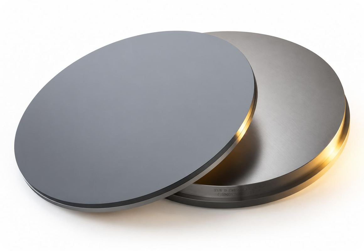
SILICON SPUTTERING TARGETS

Unique sputtering target materials.
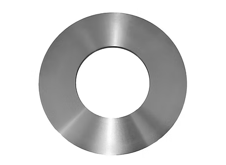
NIOBIUM

Sputtering targets for thin film.
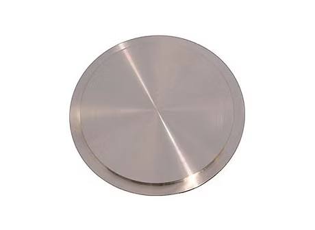
AMO

Replace your precious metals with a unique silver alloy.
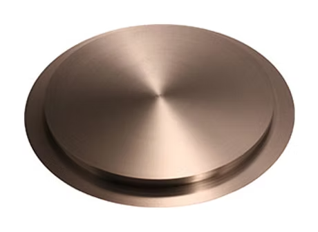
TNB

Higher index material than TiO2.
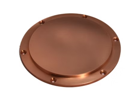
HPC

Copper coating which does not corrode.
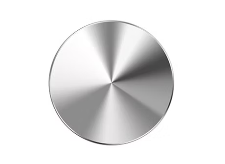
ALLOYS

Sputtering targets with precise combination of metals.
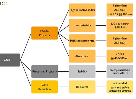
ZNB

Able to use DC for sputtering, replaces ZnS.

Let's communicate!

For further information, please contact Dirk Gertmann (dirk@spm.li, +423 788 22 27) or Michael Junker (michael@spm.li, +423 375 80 27).
Scroll to Top